Tech & AIJLCPCBHDI PCB Explained: Blind & Buried Vias | JLCPCB Industry Knowledge Series — Episode 1
HDI PCB Explained: Blind & Buried Vias | JLCPCB Industry Knowledge Series — Episode 1
Long-form2:26People & BlogsPublished Sep 7, 2026, 8:00 AM · 6w ago

Views
741
+0 views/hour
Views / hour now
0
measured 10h ago
Peak views / hour
—
First 24 hours
—
not tracked from upload
Engagement
2.0%
likes + comments / views
Likes
12
1.6% of views
Comments
3
0.40% of views
Est. ad revenue
—
channel not monetized
Checked every 24 h while the video is this age · last check 10h ago · next in 804 min. YouTube itself updates public counts with a short delay.
Avg views / day
17
since upload
vs channel median
1.0×
this video's views ÷ the channel's usual
Rank in channel
#18
of 21 tracked
Views over time
0 readings
Total views Views gained per hour
Live tracking started
The chart fills in as FameX records new readings.
Description
How do tiny devices pack so much power? HDI PCB technology.
In this viedo, we break down the core of HDI PCBs — blind vias and buried vias. Learn how these tiny structures replace traditional through-hole vias to unlock higher routing density, support fine-pitch BGA components, and enable the miniaturization of modern electronics.
📌 What you'll learn in this video:
00:00- Why Do We Need HDI
00:23- Understanding What HDI Is and Its Key Structures
00:54- How HDI Improves PCB Design Capabilities
01:10- How HDI Is Manufactured
01:28- HDI Design & Applications
01:55- Conclusion
💡 Why This Matters:
HDI technology is the backbone of compact, high-performance devices. Whether you're an engineer, a student, or just curious about how electronics work, understanding HDI gives you insight into the future of PCB design.
🔔 Subscribe to JLCPCB for more engineering insights!
👍 Like, Comment & Share if you found this helpful!
#HDI #PCBDesign #Engineering #HowItWorks #Smartphone #jlcpcb #TechExplained #STEM
Tags
JLCPCBpcbpcbapcb assemblyturnkey PCBAturnkey PCB assemblySMTSMDSMD assemblysolderinghand solderingcomponentsBGAmicrocontrollerRP2040flex PCBFR-4Rogers PCBPTFE TeflonCopper Corehigh precision PCBsilkscreenouter copperviavia-in-padPCB toleranceAOIgold fingerspcb stencilpcb prototype
Details
- Published
- Sep 7, 2026, 8:00 AM
- Length
- 2:26 (146 s)
- Format
- Long-form
- Category
- People & Blogs
- Audio language
- EN-GB
- Quality
- HD
- Captions
- No
- Made for kids
- No
- Licensed content
- No
- Video ID
- CfeyjTDp-jE
More from JLCPCB
 What Is Via-in-Pad? 👀 | A PCB Design Technique Worth Knowing306 views · 3h ago · +72/h
 Meet JLCPCB at electronica 2026 & Win Exciting Prizes!412 views · 4d ago · +3/h
 Invisible earphones, built completely from scratch. 🕵️♂️🎧3.4M views · 1w ago · +23.3K/h
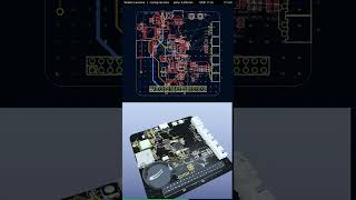 🤖 AI Hardware Dreamer Challenge – Can AI Really Build Hardware?6.2K views · 1w ago · +7/h
 This Color Came Straight from the 3D Printer! 🌈2.8K views · 1w ago · +34/h
 Get Your PCB Layout Right from Day One 🛠️3.4K views · 2w ago · +35/h
 Choosing the right PCB layer count depends on your design needs.1.1K views · 2w ago · +1/h
 "Just drill a hole, the layers connect. Easy." 😅2.7K views · 3w ago · +34/h
Statistics from the YouTube Data API, tracked by FameX. Views per hour, revenue and comparisons are FameX estimates.